IMLS Update: Analysis and New Tools
| Written by | Louise Stewart Beck |
|---|---|
| Published | 1/31/2019 |
IMLS Update: Analysis and New Tools
| Written by | Louise Stewart Beck |
|---|---|
| Published | 1/31/2019 |
 This blog post is part of a series about storage relocation and improvements that we are able to undertake thanks to a grant from the Institute of Museum and Library Services.
In the course of our work as conservators, we get some very exciting opportunities. Thanks to a partnership with Hitachi High Technologies, for the past few months the conservation lab here at The Henry Ford has had a Scanning Electron Microscope (SEM) with an energy-dispersive x-ray (EDX) spectroscopy attachment in our lab.
 What does this mean? It means that not only have we been able to look at samples at huge magnifications, but we have had the ability to do elemental analysis of materials on-demand. Scanning electron microscopy uses a beam of electrons, rather than light as in optical microscopes, to investigate the surface of sample. A tungsten filament generates electrons, which are accelerated, condensed, and focused on the sample in a chamber under vacuum. There are three kinds of interactions between the beam and that sample that provide us with the information we are interested in. First, there are secondary electrons – the electron beam hits an electron in the sample, causing it to “bounce back” at the detector. These give us a 3D topographical map of the surface of the sample. Second, there are back-scattered electrons – the electron beam misses any electrons in the sample and is drawn towards a positively-charged nucleus instead. The electrons essentially orbit the nucleus, entering and then leaving the sample quickly. The heavier the nucleus, the higher that element is on the periodic table, the more electrons will be attracted to it. From this, we get a qualitative elemental map of the surface, with heavier elements appearing brighter, and lighter elements appearing darker.
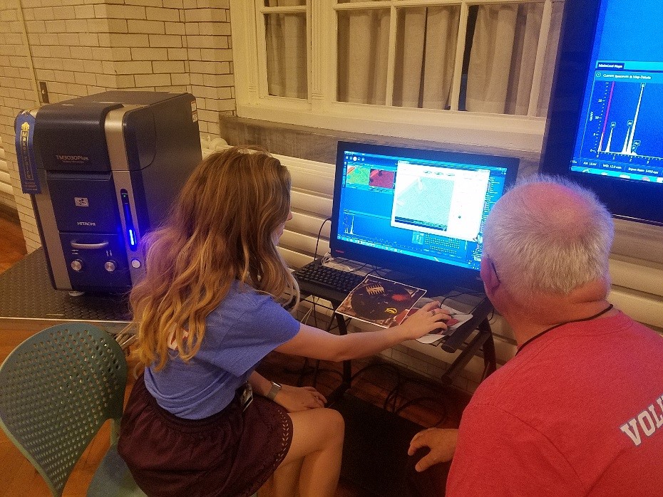
  Conservation Specialist Ellen Seidell demonstrates the SEM with Henry Ford Museum of American Innovation volunteer Pete Caldwell.
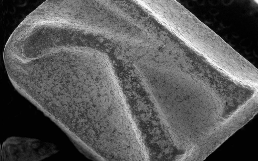
The EDX attachment to the SEM allows us to go one step further, to a third source of information. When the secondary electrons leave the sample, they leave a hole in the element’s valence shell that must be filled. An electron from a higher valence shell falls to fill it, releasing a characteristic x-ray as it does so – the detector then uses these to create a quantitative elemental map of the surface. A ‘K’ from a stamp block, as viewed in the scanning electron microscope.
The understanding of materials is fundamental to conservation. Before we begin working on any treatment, we use our knowledge, experience, and analytical tools such as microscopy or chemical tests to make determinations about what artifacts are made of, and from there decide on the best methods of treatment. Sometimes, materials such as metal can be difficult to positively identify, especially when they are degrading, and that is where the SEM-EDX shines. Take for example the stamp-block letter shown here. The letter was only about a quarter inch tall, and from visual inspection, it was difficult to tell if the block was made of lead (with minor corrosion) or from heavily-degraded rubber. By putting this into the SEM, it was possible a good image of the surface and also to run an elemental analysis that confirmed that it was made of lead. Knowing this, it was coated to prevent future corrosion and to make it safe to handle.
Elemental analysis is also useful when it comes to traces of chemicals left on artifacts. We recently came across a number of early pesticide applicators, which if unused would be harmless. However, early pesticides frequently contained arsenic, so our immediate concern was that they were contaminated. We were able to take a sample of surface dirt from one of the applicators and analyze it in the SEM. An SEM image of a dirt sample from an artifact (left) and a map of arsenic within that sample (right).
The image on the left is the SEM image of the dirt particles, and the image on the right is the EDX map of the locations of arsenic within the sample. Now that we know they are contaminated, we can treat them in a way that protects us as well as making the objects safe for future handling.
We have also used the SEM-EDX to analyze corrosion products, to look at metal structures, and even to analyze some of the products that we use to clean and repair artifacts. It has been a great experience for us, and we’re very thankful to Hitachi for the opportunity and to the IMLS as always for their continued support.
Louise Stewart Beck is the project conservator for The Henry Ford's IMLS storage improvement grant.
Keywords | |
|---|---|
Themes |
